COMPUTING
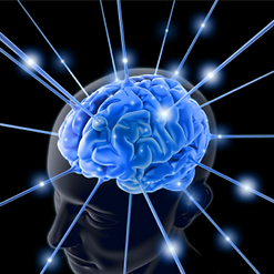
Hardware Implementation of Machine Learning
Deep learning/LLM has changed the landscape of computing hardware. Brain-inspired or neuromorphic computing aims to emulate massive parallelism of biological synapses and neurons using nanoelectronic devices so that various machine learning tasks or those that deal with abundant data (e.g., pattern recognition) can be carried out more efficiently and faster. We are one of very few research groups in the nation who have expertise in all emerging non-volatile memory device candidates, including RRAM (Resistive RAM), CBRAM (Conductive-Bridge RAM), PCM (Phase Change Memory), fRAM (ferroelectric RAM), and MRAM (Magnetic RAM). Our recent study found that silicon oxide-based RRAM and CBRAM may offer a promising device platform for IoT edge computing and GeSb-based PCM for high temperature applications such as automotive and aerospace.
Emerging Semiconductor Materials and Devices
As called for in the bipartisan CHIPS and Science Act, we proudly represent George Mason University as a leading research group for semiconductor and microelectronics. Being an active member of state-wide initiatives such as VAST (Virginia Alliance for Semiconductor Technology) and VMEC (Virginia MicroELectronics Consortium), Mason Nano Lab is conducting cutting-edge semiconductor research by leveraging state-of-the-art nanofab cleanroom facilities at the SciTech campus. Our group focuses on developing and understanding novel nanoelectronic devices. Unlike many other research groups who just put down contacts on materials for testing and call it devices, we truly engineer materials to turn them into functional micro- and nanostructures such as logic, memory, interconnect, and sensor/actuator. We are the device group who does research on device for device.
Quantum Materials and Devices
A quantum computer has recently been developed based on superconducting circuits (e.g., IBM) or neutral atoms (e.g., Atom Computing). However, the number of quantum bits (qubits) is still very few (~1,000 as of 2025), thus stopping widespread use of a quantum computer. Many research groups are looking into alternative quantum materials and devices such as silicon quantum dot, ion traps, NV-center, or topological materials. Our group is conducting research on various 2D materials that are capable of spin-based computing. Ferroelectric or phase-change 2D materials are also being researched. We also collaborate with industry to design and fabricate chip-scale RF sensor using Rb atoms in Rydberg states. We are affiliated with Mason's QSEC (quantum science and engineering center) by leading experimental quantum materials and devices research efforts.

ENERGY
Artificial Leaf
PEC (photoelectrocatalytic) water splitting is a promising, transdisciplinary approach of implementing photosynthesis by having photo-generated charge carriers involved with redox reactions in the semiconductor/electrolyte heterostructured material system. It resembles natural photosynthesis while yet producing oxygen and hydrogen at physically separated reaction sites. PEC water splitting is considered more cost-effective than fossil-based technologies for hydrogen fuel generation. We collaborate with Mason's chemistry department to both experimentally and theoretically explore the novel PEC water splitting device. We serve as the unique device research group who uses a device TCAD tool for electronic and optoelectronic simulation of artificial leaf.

High Performance Supercapacitor
Due to the intermittent nature of currently available energy harvesting technologies (e.g., photovoltaic, wind, etc.), one needs to save energy for future use. Li-ion battery is the incumbent, and researchers are trying to develop novel energy storage solutions for the future generation. Our group has expertise, skills, and backgrounds in developing micro- and nanoscale, flexible, and all solid-state supercapacitor devices. Owing to the high surface-to-mass ratio of low-dimensional nanomaterials (e.g., laser-induced graphene, reduced graphene oxide), when they are used as electrodes, energy storage devices of both high energy density and high power density can be implemented. We also possess an experimentally-benchmarked circuit model based on MATLAB/Cadence to simulate and predict the performance of these novel energy storage devices.

BIOMEDICAL
Microfluidics
Soft-lithography techniques use elastomeric stamps or polymer molds (e.g., PDMS) to create micro- and nanoscale patterns and are widely used for microfluidics research. Our group is an expert of using liquid metals to build up microfluidic devices for numerous biomedical applications. For example, we previously collaborated with UT Health Science Center at San Antonio (UTHSCSA) and US Army Institute of Surgical Research (USAISR) to fabricate high-spatial resolution tactile sensors for haptic feedback in airway management (digital intubation extender). Our group is also capable of designing and fabricating a microfluidic biosensing platform for rapid and multiplex quantification of cardiac biomarkers.

One-Stop Device for Sarcopenia
Aging is a global concern and accompanied by progressive reduction of muscle mass, which may lead to sarcopenia. Even if the prevalence of sarcopenia is almost 10% globally, it is a silent muscle disease that leads to late-stage detection. Common medical tools and instruments are limited to measuring only one component of sarcopenia, often times being expensive and not readily accessible to old adults. In collaboration with researchers at Mason's College of Public Health, our group is inventing a sarcopenia diagnosis device that integrates all components, namely muscle strength, muscle mass, and physical performance into one single platform.

Microneedle Array for Drug Delivery
The fiber-optic microneedle device is an array of hollow microneedles, capable of delivering vaccines or drugs (and light simultaneously) to increase immunogenicity. The microneedles are made of bio-degradable materials in case it fractures inside the skin. Additionally, it can be designed to penetrate the stratum corneum but short enough not to pass the epidermis layer (where the nerve cells are located), thus reducing the chances of pain, infection or injury. Our group employs state-of-the-art microfabrication techniques to develop high aspect-ratio microneedle arrays.
